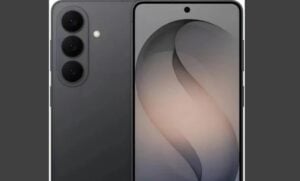
Apple develops iPhone 18 with Face ID hidden on the screen and new 24 megapixel front camera

Technology giant Apple has started the process of developing a new hardware architecture for the future line of smartphones, focusing on the complete redesign of the front panel. Engenheiros from the company are working on integrating the facial recognition system directly under the display, eliminating the need for visible cutouts on the screen. The engineering project aims to create a completely uninterrupted glass surface, changing the design standard established in recent years by the mobile device industry.
The strategic planning also involves a significant update to the front photographic hardware, which will now feature a 24 megapixel sensor, replacing the current 12 megapixel standard used in recent generations. The modification represents a technical leap aimed at capturing very high resolution images and improving augmented reality features, requiring much more robust data processing on the part of A series processors.
Structural changes in the mobile device require complex adaptations in the supply chain and manufacturing of optical components. The transition to a clean display not only changes the aesthetics, but also reshapes the internal layout of logic boards and heat dissipation systems. Entre the main technical modifications required by the new project are:
– Redesenho of the OLED panel pixel matrix to allow infrared light to pass through without distortion.
– Implementação of lenses made up of six elements in the front camera to correct chromatic aberrations.
– Atualização deep image processing algorithms to compensate for refraction caused by screen glass.
– Calibração of brightness sensors to operate efficiently even when covered by the light emission layer.
Evolution of front design on mobile devices
The smartphone market is witnessing a gradual transition in the way front sensors are accommodated in high-performance devices. The architecture started with thick edges at the ends, evolved to the wide top notch, and arrived at the floating pill-shaped cutouts adopted in more recent generations. Cada stage of this evolution required the miniaturization of critical components, such as speakers, microphones and structured light emitters.
The quest for a fully uninterrupted display represents the next stage of industrial design in the global telecommunications sector. Hiding infrared emitters and receivers requires materials with specific transparency and resistance properties, forcing the tempered glass industry to develop new alloys. The challenge is to maintain the structural integrity of the device against falls while increasing the light transmittance in millimeter areas.
The implementation of this clean architecture changes the dynamics of device use, offering a larger viewing area for media consumption, reading and browsing. The absence of visual interruptions at the top of the screen allows the operating system to redistribute status icons, notifications and interface elements in a more symmetrical way, optimizing the use of the light panel from edge to edge.
Specifications of the new 24 megapixel photo sensor
The jump in front camera resolution from 12 to 24 megapixels constitutes the biggest update to photographic hardware for front capture in the history of the company’s smartphone line. The new component captures twice as much visual information, resulting in images with a higher level of detail, more accurate textures and better performance in challenging lighting scenarios. The lens made up of six high-precision plastic elements helps direct light more efficiently to the image sensor, reducing distortions at the edges of photographs and improving continuous autofocus.


The updated hardware will work in strict synchronization with a new neural processing engine, responsible for applying real-time corrections through advanced computational photography. The system focuses on improving dynamic range, balancing areas of deep shadow and high light, in addition to refining the depth mapping used in portrait mode. The higher pixel density also allows digital cropping of the image without noticeable loss of quality, facilitating dynamic framing in corporate video calls and high-resolution live broadcasts.
Engineering behind hidden facial recognition
Under-screen facial recognition technology works by emitting tens of thousands of invisible infrared dots that map the three-dimensional geometry of the user’s face. Este mapping creates a unique mathematical mask that is compared to the encrypted data in the processor’s secure enclave.
For the system to operate correctly positioned below the display, the pixel layer of the OLED screen must have a microscopic structure hollowed out in the specific region of the sensors. The red, green and blue subpixels are rearranged to create micro-windows that allow light waves to pass through.
The infrared light must pass through the protective glass, the touch sensitivity mesh and the light emission matrix without suffering angular deviations that compromise the three-dimensional reading. Qualquer unwanted refraction can distort the mesh of points, resulting in authentication failures.
The development requires rigorous calibration via software to ignore the light interference generated by the screen itself during the biometric reading process. The system needs to differentiate between ambient light, the light emitted by the display and the reflection of the dot projector in fractions of a second.
Impact on supply chain and suppliers
The technological transition imposes new standards of rigor and quality for Asian companies responsible for manufacturing OLED panels and compact camera modules. Display suppliers have already begun adapting their cleanroom assembly lines to meet the unprecedented light transmittance requirements of the new front glass, which requires massive investments in new precision equipment.
The manufacturing process becomes substantially more complex and costly, requiring state-of-the-art lithography machinery to create the micro-apertures in the screens without affecting the pixel density visible to the human eye. Initial yield rates in the production of these panels are often low, forcing the supply chain to begin manufacturing trials months in advance to ensure the volume needed for a global launch.
Technical Challenges in Implementing Seamless Dashboard
Materials engineering faces significant physical hurdles to ensure that the area of the screen positioned over the sensors maintains exactly the same brightness, contrast and color accuracy as the rest of the display. Qualquer variation in visual quality would create a noticeable artifact, such as a pixelated square or dark spot, completely defeating the aesthetic purpose of a continuous screen. Além In addition, the 24-megapixel front camera needs to capture visible light through the same layers of material, which has historically resulted in blurry images, with internal reflections or a severe loss of contrast in early industry prototypes. The technical solution involves the application of multiple nanometer-scale anti-reflective coatings to the inner layers of the glass and the intensive use of artificial intelligence algorithms specifically trained to identify and restore the sharpness of the image captured through the physical barrier of the OLED display, cleaning up optical noise before the photo is presented to the user.
Biometric security standards in the technology sector
Maintaining the false acceptance rate at statistical levels close to one in a million remains the fundamental and non-negotiable requirement for approval of new hardware. Security engineering works to ensure that the convenience of a cutout-free design does not reduce the protection of banking data, passwords and personal information stored on the device, maintaining the certification necessary for approving contactless payments and accessing financial applications.
Veja Tambem em News (EN)

Research reveals that parents are unaware of how their children use artificial intelligence

Samsung releases new system update with new features for Galaxy Watch 4 users

Digital retail reduces the value of the Galaxy S25 5G smartphone with bank bonuses and device exchange

Amazon’s wireless CarPlay adapter has a 50% discount and high approval ratings from drivers

Zach Cregger’s new Resident Evil ignores games and focuses on an unprecedented story with new characters

Rumor suggests that Nintendo is preparing a special edition of the Switch 2 with a remake of Ocarina of Time
Apple accelerates production of the iPhone 17e and develops new Air model with dual camera system

Epic Games platform releases twelve high-budget games at no permanent cost for PC users

PlayStation 5 Pro price drop accelerates digital retail sales and eliminates global stocks

New Galaxy Watch 9 firmware appears on server and confirms progress in software development

Apple’s commemorative project tests cell phone with 1.1 millimeter edge and curved screen for 2027