Apple creates iPhone 17 Air with 5.5mm chassis and high-resistance liquid glass panel

The North American technology giant is working on the final engineering phase of a new mobile device that promises to change design standards in the global smartphone industry. The manufacturer’s central project focuses on the extreme reduction of physical measurements, involving the creation of a device with just 5.5 millimeters in profile. Esta brand establishes the equipment as the finest ever produced by the company throughout its history in the consumer electronics market.
To achieve this structural goal, engineers needed to completely restructure the hardware’s internal architecture. The development process required the creation of miniaturized components and the adoption of new materials on the assembly line, changing the way devices are designed from the drawing board. The change directly affects the arrangement of boards, sensors and power modules within the restricted chassis.
The initiative represents a paradigm shift in relation to previous launches, which prioritized increasing volume to accommodate larger batteries and multiple camera systems. The new technical approach requires millimeter precision at each stage of manufacturing, forcing suppliers and logistics partners to update their machinery to meet the new tolerance standards required by the brand.
Structural engineering and extreme size reduction
The drastic decrease in the physical dimensions of the device required a complete redesign of the main motherboard. The new component uses a copper compound coated with a special resin, a material that reduces the space occupied by essential electronic circuits without compromising electrical conductivity.
This fundamental change allows other vital components to be accommodated in an extremely constrained chassis. The relocation of internal parts was calculated by three-dimensional modeling systems to avoid any waste of millimeter space inside the device’s metal casing.
Application of liquid glass to protect the display
The device’s display incorporates technology based on liquid glass, specifically developed to offer superior resistance against direct impacts and deep scratches. The innovation replaces traditional layers of protection with a more flexible and adaptable molecular structure.
This new chemical composition is capable of absorbing severe mechanical shocks without compromising touch sensitivity or the visual quality of the images transmitted by the panel. The application of this material allows the screen to be significantly thinner than previous generations.
Independent laboratory tests indicate that the structure withstands drops from greater heights compared to common tempered glass. Improved strength reduces the need for thick protective films, which typically add unwanted bulk to a smartphone’s profile.
Advanced thermal management and processing
To deal with the heat generated by the new A19 processor, the engineering team implemented an unprecedented thermal dissipation system. The mechanism was built from a high conductivity carbon and silicon alloy.
The system works to distribute heat evenly throughout the entire rear structure of the device. Essa dispersion technique prevents the concentration of high temperatures at specific points, protecting the user’s hands and adjacent components.
Efficient thermal management is a key factor in maintaining chip performance during complex tasks. Adequate dissipation ensures that the device does not suffer performance drops caused by thermal throttling.
Preventing physical damage from overheating in such a limited indoor space was one of the biggest hurdles the research team overcame. Sensores internal monitors temperature in real time to adjust processing load as needed.


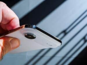
Modifications to the photographic module and light capture
Unlike conventional models that feature multiple photographic sensors on the back, the new design adopts a single camera module. The technical and design decision aims to save physical space at the top of the device, an area that is traditionally occupied by ultrawide, telephoto lenses and depth sensors. The module alignment has also undergone significant changes, being positioned centrally to optimize weight distribution and improve ergonomics during daily handling of the equipment.
Despite the reduction in the number of lenses available to the user, the main sensor has been vastly improved to capture a greater amount of light and record precise details in low-light environments. The component uses advanced machine learning-based image processing algorithms to compensate for the absence of secondary photographic hardware. The protective structure of the lens was reinforced with the same liquid glass material used in the front display, ensuring uniform resistance of the device.
Development of high energy density batteries
Continuous power supply for the ultra-thin device relies solely on a new generation of high-density batteries, designed from the ground up to store more charge in physically smaller and thinner cells. The record thickness of 5.5 millimeters makes the use of traditional lithium-ion batteries impossible, forcing the adoption of alternative chemical compounds that offer greater energy efficiency per square millimeter. The physical structure of the battery has been shaped asymmetrically to fill all voids around the motherboard and antenna modules, maximizing total capacity without expanding the volume of the metal chassis. Essa precision engineering guarantees enough autonomy for a full day of moderate use, meeting the constant connectivity demands of modern consumers without sacrificing the aesthetic proposal of the project.
Adaptations to global supply chain machinery
The large-scale production of this model places rigorous demands on the global supply chain, requiring precision machinery unheard of in Asian assembly plants. Fornecedores of optical components, glass panels and printed circuits needed to update their production lines on an emergency basis to meet the new millimeter tolerance standards established by the North American manufacturer.
Rigorous physical testing protocols in factories
Assembling a device with such narrow margins for error requires a highly controlled manufacturing environment. The industrial facilities responsible for final production were equipped with laboratory-grade air filtration systems to prevent contamination.
Automated machines apply controlled torsional and bending forces to the smartphone’s body to ensure the rigidity of the ultra-thin structure. Dispositivos that present any millimeter deviation in relation to the original design are immediately discarded from the main line.
Commercial positioning in the premium handset segment
The introduction of a smartphone with such a low profile sets a new standard for industrial design in the mobile technology sector. The move forces competing companies to reevaluate their own research and development schedules for the coming semesters. Advances in chip miniaturization have reopened the possibility of focusing on ultra-thin aesthetics, something that had been left on the back burner by the industry.
The price positioning of this model directly reflects the high research costs, specialized machinery and exclusive materials used in manufacturing. The strategy targets the product at a specific niche of consumers who value extreme portability and aesthetic innovation above the photographic versatility offered by multiple lens systems present in other models from the same brand.
Distribution logistics and equipment calibration
The partner assembly lines have already started the production testing phase in small batches to calibrate the precision laser equipment. The pace of manufacturing will be gradually staggered over the next few months to avoid severe logistical bottlenecks. Rigorous planning ensures that the necessary volume of miniaturized components is available to meet initial demand at the time of official launch in the main international technology markets.
Veja Tambem em News (EN)

Research reveals that parents are unaware of how their children use artificial intelligence

Samsung releases new system update with new features for Galaxy Watch 4 users

Digital retail reduces the value of the Galaxy S25 5G smartphone with bank bonuses and device exchange

Amazon’s wireless CarPlay adapter has a 50% discount and high approval ratings from drivers

Zach Cregger’s new Resident Evil ignores games and focuses on an unprecedented story with new characters

Rumor suggests that Nintendo is preparing a special edition of the Switch 2 with a remake of Ocarina of Time
Apple accelerates production of the iPhone 17e and develops new Air model with dual camera system

Epic Games platform releases twelve high-budget games at no permanent cost for PC users

PlayStation 5 Pro price drop accelerates digital retail sales and eliminates global stocks

New Galaxy Watch 9 firmware appears on server and confirms progress in software development

Apple’s commemorative project tests cell phone with 1.1 millimeter edge and curved screen for 2027