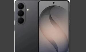
Apple creates new ultra-thin smartphone with 5.5 millimeters thickness and liquid glass screen

The mobile device industry is undergoing a restructuring of its design standards with the development of new equipment focused on extreme size reduction. The North American manufacturer’s recent project establishes the creation of a device just 5.5 millimeters thick, marking a significant departure from previous generations that prioritized larger batteries and protruding camera modules. Esta paradigm shift requires complete redesign of internal hardware architecture to accommodate high-performance components in a severely constrained physical space.
To make this unprecedented thickness possible, engineers needed to abandon traditional assembly methods and adopt cutting-edge materials that guaranteed the structural integrity of the device. Reducing the device’s profile not only affects aesthetics, but changes the way heat dissipation, image capture and screen durability are managed in daily use.
The development of this equipment is based on specific technological pillars that work together to avoid mechanical and thermal failures. The combination of new chemical compounds in the screen and metal alloys in the chassis allows the device to maintain the rigidity necessary to withstand the pressure of carrying it in pockets and bags, a historical problem faced by excessively thin devices in the past.
- Implementation of aerospace-grade titanium alloy chassis for maximum torsional resistance.
- Front panel equipped with liquid glass technology capable of molecular regeneration against microcracks.
- Passive cooling system using high-density graphene sheets and a microscopic vapor chamber.
- Periscope camera module mounted horizontally to eliminate rear bulge.
- Dedicated neural processing unit for executing local machine learning tasks.
Aerospace titanium-based structural engineering
The main challenge in building a 5.5mm device is preventing structural flexion, a phenomenon that can cause irreversible damage to the logic board and screen. To address this issue, the device’s main structure is machined from solid blocks of aerospace-grade titanium.
This material replaces the aluminum and stainless steel used in conventional production lines, offering a substantially higher weight-resistance ratio. Titanium allows the edges of the device to be extremely thin without compromising the ability to absorb direct mechanical impacts.
The internal architecture of the chassis was redesigned with strategic reinforcements at points of greatest mechanical stress. Esta force distribution ensures that the pressure exerted in the center of the device is dissipated towards the ends, protecting the most sensitive internal components against accidental twisting.
Molecular innovation with liquid glass panel
The new device’s display surface incorporates liquid glass technology, a chemical formulation that changes the way the panel responds to surface damage. Diferente than traditional tempered glass, this material has a polymer structure that maintains a certain mobility at a molecular level. Quando micro-scratches caused by friction with keys or coins occur, the panel’s molecules tend to slowly reorganize over time, filling the cracks and restoring the screen’s original optical clarity. Este self-regeneration process is accelerated by slight variations in temperature during normal use of the device.
The adoption of liquid glass also directly contributes to the final thickness of 5.5 millimeters. By eliminating the need for multiple layers of rigid protection over the OLED display, engineers were able to shave crucial fractions of a millimeter off the front panel. Além of regeneration capacity, the material has an optimized refractive index, which allows the light emitted by the organic diodes to cross the surface with less dispersion, resulting in higher brightness levels without the need to increase battery power consumption.
Advanced passive thermal management
Heat dissipation represents the biggest physical obstacle in ultra-thin profile electronics. Sem room for thick copper heatsinks, heat generated by the central processor can cause rapid component degradation.


The solution found involves a multi-layer passive cooling system. Folhas of high thermal conductivity graphene are positioned directly on the highest processing chips, pulling heat in a directional manner.
Working in conjunction with graphene, an ultra-thin vapor chamber was developed specifically for this chassis. Esta chamber contains a microscopic amount of liquid that evaporates as it absorbs heat, moving to cooler areas where it condenses and returns to a liquid state.
This continuous cycle of phase change maintains the operating temperature within safe limits. The efficiency of this system ensures that the device does not suffer drastic performance reductions from thermal throttling during demanding tasks.
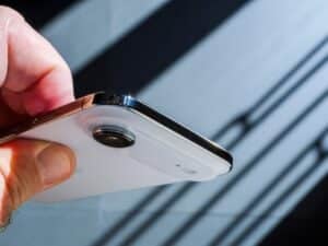
Chassis-flush photographic architecture
The rear design of the equipment stands out for the total absence of the traditional camera bump. Para accommodate high-resolution sensors in a 5.5mm body, the optical system has been rotated by ninety degrees.
Periscopic lens technology uses prisms to reflect captured light along the horizontal axis of the phone. Isso allows the inclusion of a complex set of lenses for optical zoom without any part of the module exceeding the thickness of the rear glass panel.
Integrated neural processing for artificial intelligence
The device’s logic board houses an Unidade of Processamento Neural designed to perform up to 120 trillion operations per second, a key requirement for the new generation of artificial intelligence tasks. The ability to process complex data directly on local hardware, without the need to send information to cloud servers, changes the dynamics of device use. Esta architecture guarantees absolute privacy for the user in functions such as continuous voice recognition, simultaneous language translation without an internet connection and semantic analysis of photographs. Local processing also dramatically reduces the latency of operating system responses, allowing machine learning algorithms to adjust battery power consumption in real time based on the owner’s daily usage patterns. The deep integration of this neural unit with the image sensors enables the application of advanced computational photography, correcting lighting and focus imperfections at the exact moment of capture, compensating for the physical limitations imposed by the reduced size of the lenses in the ultra-thin chassis.
Summary of hardware innovations
The consolidation of these technologies establishes new parameters for the engineering of high-end mobile devices. The integration of miniaturized components requires absolute precision on the assembly line.
- Structural profile strictly maintained at 5.5 millimeters.
- Precision machining using aerospace titanium alloys.
- Front panel with self-healing liquid glass polymers.
- Phase change cooling system in a vapor chamber.
- Periscopic photographic module fully embedded in the chassis.
- Neural processor with a capacity of 120 trillion operations per second.
Veja Tambem em News (EN)

Research reveals that parents are unaware of how their children use artificial intelligence

Samsung releases new system update with new features for Galaxy Watch 4 users

Digital retail reduces the value of the Galaxy S25 5G smartphone with bank bonuses and device exchange

Amazon’s wireless CarPlay adapter has a 50% discount and high approval ratings from drivers

Zach Cregger’s new Resident Evil ignores games and focuses on an unprecedented story with new characters

Rumor suggests that Nintendo is preparing a special edition of the Switch 2 with a remake of Ocarina of Time
Apple accelerates production of the iPhone 17e and develops new Air model with dual camera system

Epic Games platform releases twelve high-budget games at no permanent cost for PC users

PlayStation 5 Pro price drop accelerates digital retail sales and eliminates global stocks

New Galaxy Watch 9 firmware appears on server and confirms progress in software development

Apple’s commemorative project tests cell phone with 1.1 millimeter edge and curved screen for 2027