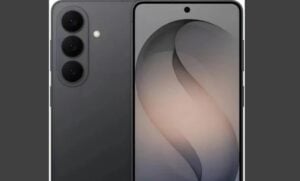
New Samsung smartphone appears in performance tests with 8 GB of RAM and deca-core processor
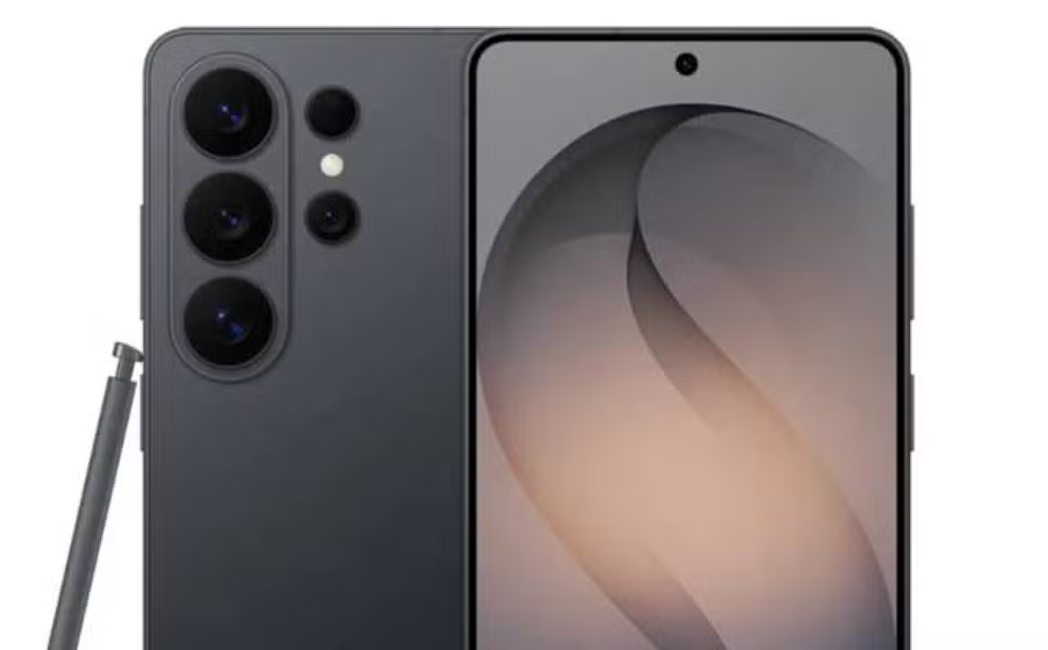
The development of the South Korean manufacturer’s next generation of high-performance mobile devices has reached a crucial phase of laboratory testing and hardware validation. A new device, identified by the model code SM-S741U, had its technical specifications detailed after registrations on specialized computing performance evaluation platforms. The data extracted from the reports points to significant advances in processing architecture and native software integration.
The appearance of the equipment in benchmark databases signals that the product engineering cycle is at an advanced stage, surpassing the initial prototyping phases. The information collected reveals the use of proprietary hardware, consolidating the strategy of diversifying components into equipment aimed at balancing cost and benefit. The score obtained reflects an optimization specifically targeted for multitasking and intensive graphics processing.
The device achieved 2,426 points in single-core tests and 8,004 points in multi-core evaluations, numbers that place it in a prominent position in the category. The random access memory configuration identified in the leak is 8 GB, setting a standard of operational efficiency for the premium intermediary line. The technical set aims to serve consumers who require constant fluidity when transitioning from heavy applications.
Internal architecture and division of processing cores
The central core of the equipment will be composed of a ten-core processing unit, organized in a complex structure that balances raw performance and energy savings. The processor features a high-speed main core operating at 3.30 GHz. Este The primary component is solely responsible for handling the operating system’s most demanding tasks and peak calculations.
Accompanying the main core, the hardware has two medium cores configured to run at a frequency of 2.75 GHz. Esta intermediate layer acts directly on medium complexity activities, relieving the processing load of the main unit. Strategic division allows for superior thermal management during extended sessions of continuous use.
For background processes that require less energy demand, the chip integrates five 2.36 GHz cores and two base cores with a frequency of 1.80 GHz. Esta deca-core configuration reinforces the use of an advanced variant of the brand’s proprietary processor family. The intelligent distribution of tasks between the different cores maximizes battery life throughout the day.
The choice of internal hardware determines the overall fluidity of the interface and the device’s immediate responsiveness to user commands. The technical arrangement focuses on avoiding thermal throttling, a critical factor in maintaining performance in competitive electronic games and recording videos in very high resolution without frame drops.
Advanced graphics performance with integrated visual technology
The presence of the Xclipse 950 graphics processing unit confirms the heritage of visual technologies previously restricted to the most expensive equipment in the company’s portfolio. Este component, developed from strategic partnerships focused on visual computing architecture, provides support for advanced rendering technologies. The ability to render dynamic reflections, variable shading and realistic lighting on the device’s screen raises the bar in the mobile device category. The convergence between graphics hardware and operating system instructions guarantees a stable usage experience, even in scenarios of high thermal demand and continuous processing of complex textures.
The architecture based on cutting-edge technology allows the execution of professional tasks, such as video editing in multiple channels and the rendering of three-dimensional models, with greater speed than its predecessors on the same assembly line. The graphics unit is optimized to work in sync with new hardware acceleration application programming interfaces provided by system developers. Esta synergy between the internal components positions the device as a highly competitive option compared to direct competitors that use graphics chips supplied by third parties, guaranteeing absolute fluidity in the frame transition and in the panel’s tactile response.
Software integration and extended update cycle
The direct mention of the operating system Android 17 as the native platform of the tested prototype reveals very advanced software engineering planning. The manufacturer already operates with preliminary versions of the source code to guarantee the total stability of its customized interface before mass production. The presence of such an advanced version of the system reinforces the structural commitment to the longevity of the equipment.


The joint development of the hardware with the new version of the operating system allows for extremely fine adjustments in memory allocation management. Standby battery consumption receives direct optimizations through efficient communication between the central processor and software protocols. Deep integration results in much more intelligent and autonomous system resource management.
Equipment in this specific category usually receives software support for an extended period, guaranteeing monthly security packages and new interface features for several consecutive years. Consumidores Those looking for a long-lasting device will find these technical specifications a solid argument for purchasing, minimizing the financial and environmental need for frequent mobile device changes.
Component strategy and production cost optimization
Information parallel to the performance leak suggests strategic revisions to the global supply chain to optimize display panel production costs. Mudanças suppliers of organic light-emitting screens allow us to maintain competitive retail prices without sacrificing color fidelity and visual quality. The industry goal is to standardize variable refresh rates and brightness levels for use in direct sunlight.
The search for new commercial partners is part of a comprehensive logistics plan to mitigate the impacts of exchange rate fluctuations and semiconductor prices on the international market. By diversifying supply sources for essential internal modules, the manufacturer acquires greater margin of maneuver in large-scale negotiations, resulting in a final product with cutting-edge specifications and strictly controlled manufacturing costs.
Network connectivity and digital payments infrastructure
The set of leaked specifications also points to the integration of next-generation modems, ensuring full support for the fastest telecommunications networks available globally. The antenna architecture was redesigned to optimize signal reception in high-density urban areas, reducing latency in mobile data connections. Support for new local wireless standards ensures significantly higher file transfer rates.
The device’s security infrastructure includes dedicated chips for the encrypted storage of sensitive data, essential for the operation of digital wallets. Proximity communication technology has been improved to ensure faster and safer financial transactions at payment terminals. Este hardware-based security level meets the stringent requirements of international financial institutions.
History of the product line and acceptance by the consumer public
Since the introduction of the first model focused on bringing together the features most praised by users at a more affordable acquisition cost, the manufacturer uses direct and quantifiable feedback from its community to define the engineering priorities of each new generation. Maintaining a long-lasting battery, combined with efficient energy management systems, consistently appears at the top of consumer demands in market research and specialized discussion forums. The integration of artificial intelligence resources applied to computational photography, simultaneous translation and daily productivity has become a central and non-negotiable pillar of the experience offered. Choosing a proprietary chipset over off-the-shelf options often generates heated technical debates, but constant improvements in manufacturing lithography and thermal dissipation design demonstrate a clear maturation of in-house production. The long-term corporate objective is to prove, through real usage metrics, that the stability and performance of the new processors operate at exactly the same level as the best global competitors, consolidating the multi-core architecture as a definitive solution for intense daily use and ensuring that the device maintains its technological relevance throughout its planned useful life cycle.
Monitoring of certifications and next steps for the manufacturer
The global technology market continuously monitors new registrations with international telecommunications and electronic security regulatory bodies. Estas Future mandatory certifications are essential procedures to confirm additional technical details about the exact rated battery capacity, maximum supported charging speeds, and full optical specifications of the rear camera array before any official announcement by the company.
Veja Tambem em News (EN)

Research reveals that parents are unaware of how their children use artificial intelligence

Samsung releases new system update with new features for Galaxy Watch 4 users

Digital retail reduces the value of the Galaxy S25 5G smartphone with bank bonuses and device exchange

Amazon’s wireless CarPlay adapter has a 50% discount and high approval ratings from drivers

Zach Cregger’s new Resident Evil ignores games and focuses on an unprecedented story with new characters

Rumor suggests that Nintendo is preparing a special edition of the Switch 2 with a remake of Ocarina of Time

Apple accelerates production of the iPhone 17e and develops new Air model with dual camera system

Epic Games platform releases twelve high-budget games at no permanent cost for PC users

PlayStation 5 Pro price drop accelerates digital retail sales and eliminates global stocks

New Galaxy Watch 9 firmware appears on server and confirms progress in software development

Apple’s commemorative project tests cell phone with 1.1 millimeter edge and curved screen for 2027