Apple develops iPhone 17 Air with liquid glass screen and unprecedented thickness of 5.5 millimeters
The electronics manufacturer based in Cupertino has begun the process of developing a new mobile device that promises to change the physical standards of the smartphone industry. The current project involves the creation of a device with extremely small dimensions, focusing on a completely redesigned internal architecture to accommodate high-performance components in a minimum space. Engenheiros of the company work to overcome traditional physical barriers, seeking to integrate advanced technologies without compromising the structural integrity of the equipment.
The hardware team’s main focus is on restructuring the logic board and power modules, which needed to be miniaturized to fit into the new chassis. Reducing internal volume requires a different approach to the allocation of each microchip, sensor and connector, eliminating any unused space within the device. Essa paradigm shift in cell phone construction requires new methods of welding and fastening parts, as well as stronger materials to prevent twisting or breaking during daily use.
To enable the continuous operation of the operating system and demanding applications, the company needed to rethink the way heat is dissipated. The extreme proximity between the main processor, battery and screen creates a complex thermodynamic challenge, requiring passive cooling solutions that do not rely on fans or moving components. The use of specific metal alloys and chemical compounds with high thermal conductivity has become essential to maintain the operating temperature within the safe limits established by international electronic safety standards.
The production line also undergoes rigorous adaptations to deal with the initial fragility of components before final assembly. Máquinas with millimeter precision were calibrated to handle parts that are the thickness of a few sheets of paper, operating in environments with strict control of particles suspended in the air. The level of automation has reached a level where direct human intervention in the assembly of the main circuits is practically zero, guaranteeing a failure rate close to zero during large-scale manufacturing.
Engineering focuses on extreme reduction of physical measures
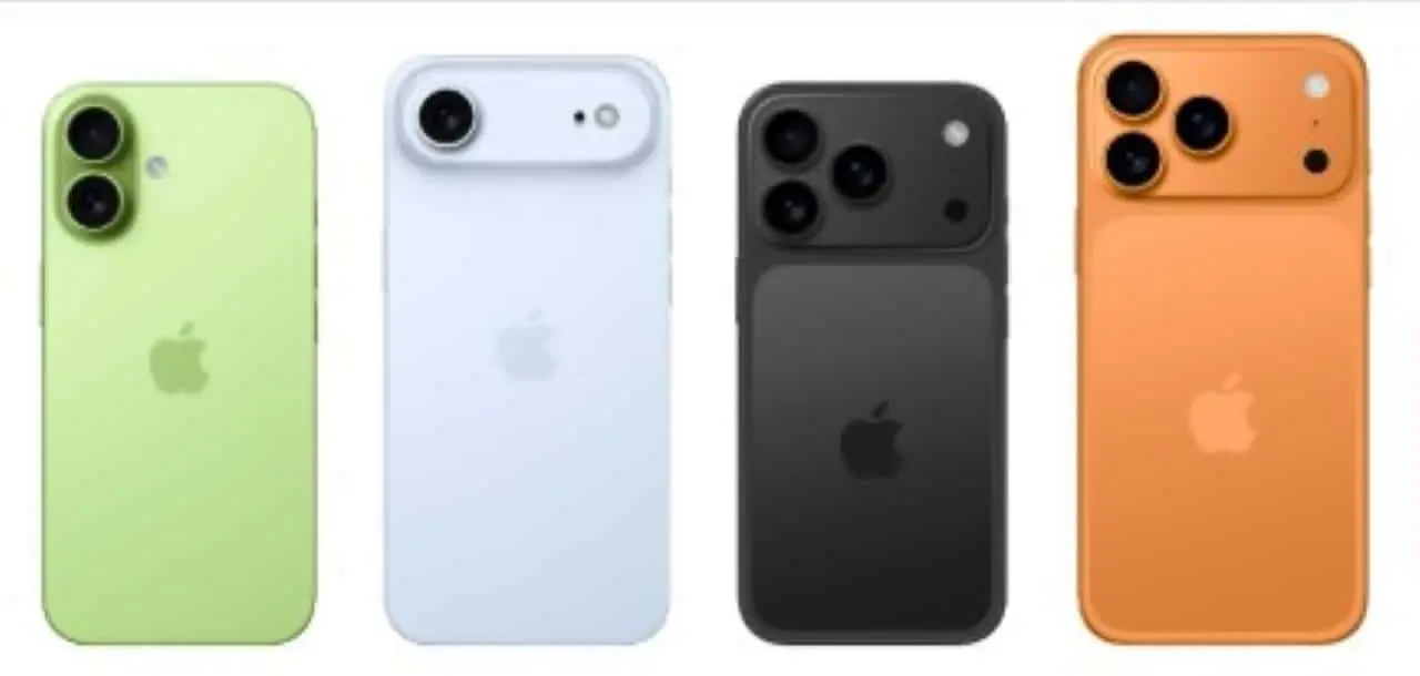
The new model reaches a thickness of exactly 5.5 millimeters, making it one of the thinnest devices ever designed in the history of mobile communication. Essa measure represents a drastic cut from previous generations, requiring parts suppliers to adapt their own production lines to deliver camera modules, speakers and vibration motors with ultra-low profiles. The outer casing acts not only as protection, but as an integral part of the heat dissipation system.
The removal of physical ports and traditional mechanical buttons contributes to saving internal space and increases chassis rigidity. Sensores pressure and capacitive surfaces replace physical volume and power switches, sending direct electrical signals to the controller board. Essa Transitioning to a solid-state design eliminates entry points for dust and liquids and removes mechanical components susceptible to natural wear and tear over consumer usage.
Liquid glass technology integrates front panel
The device’s display surface uses technology based on liquid glass, a synthetic material that offers superior optical properties and greater structural flexibility. Esse compound allows the screen to absorb direct impacts more efficiently, distributing the kinetic force across the entire length of the front panel instead of concentrating it at a single point of rupture. The transparency of the material guarantees the passage of light from the emitting diodes with minimal loss of brightness or color distortion.
The manufacturing process for this glass involves rapidly cooling molten polymers under vacuum conditions, creating a disordered molecular structure that prevents cracks from propagating. The touch-sensitive layer is printed directly on the bottom of this glass, eliminating the need for thick stickers that normally separate the display from the capacitive sensor. Essa direct integration reduces the total thickness of the display module by fractions of a millimeter crucial to the design.
The new screen’s haptic response has been adjusted by software algorithms to compensate for the changed rigidity of the front material. The operating system recognizes subtle variations in the pressure exerted by the user’s fingers, differentiating intentional touches from accidental bumps on the device’s ultra-thin edges. Sensores ambient light and infrared emitters for facial recognition operate through microperforations invisible to the naked eye, maintaining the visual continuity of the liquid glass surface.
Thermal dissipation system uses advanced graphene
Temperature management inside the 5.5mm chassis relies on a high-density graphene sheet that covers most of the logic board. Graphene acts as a thermal highway, capturing the heat generated by the central processor and graphics chip, and quickly spreading it towards the device’s aluminum edges. Essa dispersion prevents the formation of localized hot spots that could damage the battery or cause discomfort to the user’s hands during intense processing.
In addition to the graphene, a microscopic vapor chamber was inserted between the battery and the screen, containing a refrigerant fluid that changes physical state as the temperature increases. Quando the processor reaches a specific thermal threshold, the fluid evaporates, absorbing the thermal energy, and travels to cooler areas of the chassis, where it condenses and returns to a liquid state. Esse Continuous cycle of evaporation and condensation occurs in a space just 0.3 millimeters thick.
Leia Também

Financial analysis indicates that GTA 6 generated US$1 billion in the first hour of pre-sales

George Russell secures second Formula 1 triumph and leads Austrian GP after controlling Verstappen and Antonelli

Air crash in France kills 11 people on parachuting school aircraft
Power management software works in conjunction with thermal hardware, monitoring dozens of temperature sensors spread across the device in real time. If passive dissipation is not enough to contain heat during heavy tasks such as video rendering or artificial intelligence processing, the system dynamically reduces the processor frequency. Essa technique, known as thermal throttling, is applied gradually so as not to cause sudden interruptions in the functioning of applications.
The external metal structure receives a special anodizing treatment that increases its ability to radiate heat to the external environment. The wireless communication antennas, strategically positioned at the ends of the device, are thermally isolated to ensure that the heat dissipated by the chassis does not interfere with the reception of radio signals. The balance between thermal conductivity and electrical insulation was achieved through exhaustive computer simulations before the production of the first physical prototypes.
Logic board and battery receive unprecedented miniaturization
The main printed circuit board has been redesigned using a stacked format, where multiple layers of silicon are connected vertically via microscopic vias. Essa three-dimensional architecture allows the processor, random access memory and solid-state storage to occupy a significantly smaller area compared to traditional flat boards. The transistor density was increased to the limit of current lithography, reducing the distance that electrical signals need to travel and, consequently, reducing energy consumption and latency in communication between the system’s critical components. Electromagnetic isolation between layers prevents radio frequency interference from affecting processor performance.
The device’s power supply is based on a new chemical formulation that increases the density of energy stored per cubic centimeter. The battery cells are manufactured in a moldable format, filling the irregular spaces left by the logic board and camera module within the ultra-thin chassis. The anode material has been enriched with silicon compounds, allowing greater retention of lithium ions during charge and discharge cycles, which compensates for the reduction in the battery’s total physical volume. Circuitos protection devices integrated directly into the battery casing monitor voltage and current at a cellular level, preventing overloads and ensuring chemical stability even under conditions of extreme use and variable temperatures.
Unified photo module optimizes image capture
The optical capture system has been consolidated into a single rear module that houses multiple overlapping lenses, replacing the traditional approach of separate cameras for different focal lengths. A precision mechanism moves the glass elements internally, changing the field of view and optical zoom level without the need for protruding lenses on the outside of the device. The main image sensor has enlarged pixels, capable of capturing a greater number of photons in low-light environments, reducing digital noise in night photographs. Optical image stabilization works in three distinct axes, using miniature gyroscopes to detect the tremors of the user’s hands and move the sensor in the opposite direction in fractions of a second. The image signal processor, integrated directly into the core chip, applies computational photography algorithms instantly, fusing multiple exposures to create a final image with wide dynamic range and sharp detail in shadow and highlight areas. The outer lens has a vapor-applied anti-reflective coating, minimizing light artifacts and unwanted reflections when shooting direct light sources. Autofocus uses phase detection on all pixels of the sensor, ensuring fast locking on moving objects, regardless of the lighting conditions of the scene.
Robotic assembly ensures precision on an industrial scale
Device assembly takes place in industrial facilities classified as aerospace-grade cleanrooms, where air filtration removes microscopic particles that could compromise internal circuits. Braços Robotics equipped with computer vision systems perform component alignment with tolerances measured in microns, ensuring that the liquid glass screen fits perfectly into the metal chassis. The application of structural adhesives and water sealants is done by automated dispensers that control the exact volume of material needed for each joint.
The quality inspection process uses X-ray and computed tomography scanners to check the integrity of internal welds and the absence of air bubbles in the battery before the device is definitively sealed. Cada unit undergoes thermal and mechanical stress tests in environmental simulation chambers, where they are subjected to rapid variations in temperature and pressure. The data collected during these tests feeds machine learning algorithms that continually adjust the parameters of assembly machines on the production line.
Structure combines titanium and aerospace aluminum
The structural integrity of the 5.5mm chassis is ensured by the use of a titanium alloy on the outer edges, fused to an aerospace-grade aluminum internal frame. Titanium provides superior resistance against scratches and direct side impacts, while the aluminum skeleton acts as the main thermal conductor and lightweight support for the logic board and battery. The union of these two metals occurs through a solid-state diffusion process under high pressure and temperature, creating a single, continuous piece that withstands daily stresses without suffering permanent deformation.